Chapter 9
Output Stages and Power Amplifiers
This chapter is concerned with the study of output stages and power amplifiers. Output stages are used to supply large amounts of power to a load with very little signal distortion and with maximum efficiency. Power amplifiers are simply amplifiers with a high-power output stage. In this chapter we shall demonstrate how one utilizes Spice to compute the various performance measures of an output stage. This will include such measures as power efficiency and harmonic distortion. In addition, we shall also investigate the role of short-circuit protection circuits that are commonly incorporated into the circuit of an output stage.
9.0 Emitter-Follower Output Stage
In Fig. 9.1 we display an emitter-follower output stage biased with a constant current source of Ibias » (15-0.7)/5k = 2.86 mA realized by transistors Q2, Q3 and resistor R. The output terminal of this stage is connected to a load resistance of 1 k-ohm. With the aid of Spice, we would like to determine the transfer characteristic of the emitter-follower assuming that each transistor is modeled after the widely available commercial 2N2222A npn transistor. The Spice input listing of the emitter-follower shown in Fig. 9.1 is given below in Fig. 9.2. A DC sweep of the input voltage source is requested to be performed between -20 V and +20 V. Although this particular voltage sweep extends beyond the power supply limits of the output stage, it is intended to highlight the saturation limits of the emitter-follower.
Submitting the input file listed in Fig. 9.2 to Spice results in the emitter-follower transfer characteristic shown in Fig. 9.3. As is evident from these results the output voltage saturates at --3.25 V for inputs below -2.7 V, and saturates at +14.9 V for input levels beyond +15.6 V. This output stage also exhibits an input offset voltage of +0.67 V. The slope of the transfer characteristic within the linear region of operation is very nearly unity.
It is interesting to note that the lower saturation limit of the output voltage is somewhat greater than that predicted by the simple equation IbiasRL. Specifically, according to this simple expression, the lower saturation limit should be -2.86 mA x 1k Ohm = -2.86 V, instead of the simulation result of -3.25 V. The reason for this deviation from the simple theory is due to the fact that the output current of the current source Q2 varies with output voltage. This is confirmed by the plot of the collector current of Q2 versus the output voltage vo, shown in Fig. 9.4. (This is found by sweeping the voltage that appears across the collector-emitter terminals of Q2 and monitoring its collector current). Notice that at an output voltage of -14.3 V, the collector current of Q2 equals 2.86 mA and increases with increased output voltages.
|
Fig. 9.1: An emitter-follower output stage with current-source bias.
|
A Class A Output Stage
** Circuit Description ** * power supplies Vcc+ 1 0 DC +15V Vcc- 2 0 DC -15V * input signal source Vi 3 0 DC 0V * output transistor Q1 1 3 4 Q2N2222A * load resistance Rl 4 0 1k * bias circuit R 0 5 5k Q2 4 5 2 Q2N2222A Q3 5 5 2 Q2N2222A * transistor model statement for the 2N2222A .model Q2N2222A NPN (Is=14.34f Xti=3 Eg=1.11 Vaf=74.03 Bf=255.9 Ne=1.307 + Ise=14.34f Ikf=.2847 Xtb=1.5 Br=6.092 Nc=2 Isc=0 Ikr=0 Rc=1 + Cjc=7.306p Mjc=.3416 Vjc=.75 Fc=.5 Cje=22.01p Mje=.377 Vje=.75 + Tr=46.91n Tf=411.1p Itf=.6 Vtf=1.7 Xtf=3 Rb=10) ** Analysis Requests ** .DC Vi -20V +20V 100mV ** Output Requests ** .PLOT DC V(4) .Probe .end
Fig. 9.2: The Spice input file for computing the transfer characteristics of the emitter-follower output stage shown in Fig. 9.1.
|

|
Fig. 9.3: The transfer characteristics of the emitter-follower circuit shown in Fig. 9.1. As is evident, the output voltage can swing between --3.25 V and 14.9 V without experiencing significant distortion.
|
Fig. 9.4: The dependence of the collector current of Q2 on the output voltage vo.
|


To better understand the behavior of the voltage-follower output stage, let us consider applying several sine-wave signals of 1 kHz frequency having various amplitudes to the input of the circuit. In this way we can visualize the expected output signals from the emitter-follower circuit as one would see in the laboratory using a function generator and an oscilloscope. More specifically, let us consider applying three different sinewaves having amplitudes of 1 V, 2.7 V and 10 V to the input of the amplifier. According to the transfer characteristic of the emitter-follower circuit shown in Fig. 9.3, the 1 V sinewave and the 2.7 V sine-wave signal should pass undistorted (although, the 2.7 V signal should just barely pass undistorted). On the other hand, the 10 V signal should become clipped on the negative portion of the output waveform. To see this using Spice, we use for each input level a modified version of the Spice deck shown in Fig. 9.2 in which the input voltage source statement is replaced by one that describes a sine-wave input. For example, in the case of the 1 V input signal, the Spice statement would appear as follows:
Vi 3 0 sin ( 0V 1V 1kHz ).
Similar statements can be written for the other two input levels. In addition to this, the following two Spice statements are included in each Spice deck to compute the transient response of the circuit over three periods of the input signal:
|
.TRAN 10us 3ms 0ms 10us .PLOT TRAN V(4). |
One hundred points per period of the output waveform will be collected and plotted. The three Spice decks corresponding to the three input levels are concatenated into one file for easy comparison of the final results.
On completion of the Spice analysis, the output of the emitter-follower for the three different input signals are shown plotted in Fig. 9.5. These results confirm that for sine-wave inputs less than 2.7 V, the output waveform does not reveal any obvious distortion. On the other hand, for an input sinewave of 10 V peak, the negative portion of the output sinewave is clipped at a level of -3.25 V.
|
Fig. 9.5: The output voltage waveform of the voltage-follower circuit of Fig. 9.1 for three different input levels: 1 V, 2.7 V and 10 V. Excessive voltage clipping occurs on the negative portion of the output voltage waveform corresponding to an input amplitude of 10 V.
|
Fig. 9.6: Several waveforms associated with the emitter-follower circuit of Fig. 9.1 when excited by a 2.7 V, 1 kHz sinusoidal signal. The top graph displays the voltage across the load resistance, the next graph displays the collector-emitter voltage of Q1, the third graph from the top displays the collector current of Q1, and the bottom graph displays the instantaneous power dissipated by Q1.
|


Other waveforms associated with the emitter-follower as calculated by Spice are shown in Fig. 9.6. The input to this circuit is a 2.7 V sine-wave signal of 1 kHz frequency (the largest input signal that can be applied to the emitter-follower circuit before distortion sets in). The Spice deck for this analysis is identical to that just described; only the plot command is changed according to:
.PLOT TRAN V(4) V(1,4) I(Vcc+).
The top graph shows the voltage waveform that appears across the load resistance. The output signal is sinusoidal with a peak value of 2.62 V riding on a DC level of -0.614 V. The second and third graph from the top display both the collector-emitter voltage and the collector current of transistor Q1, respectively. Both of these waveforms appear sinusoidal with amplitudes of 2.62 V and 2.703 mA, respectively. The average value of the voltage waveform appearing between the collector and emitter terminals is 15.61 V. Similarly, the average value of the collector current is 2.73 mA. The bottom-most graph displays the instantaneous power dissipated by Q1. This waveform was obtained by multiplying together the collector current and collector-emitter voltage of Q1 using Probe. The peak value associated with this waveform is 70.58 mW and its average value is about 40 mW.
|
Fig. 9.7: A Class B output stage. |
Example 9.1: Class B Output Stage
** Circuit Description ** * power supplies Vcc+ 1 0 DC +23V Vcc- 2 0 DC -23V * input signal source Vi 3 0 sin ( 0V 17.9V 1kHz ) * output buffer Qn 1 3 4 NA51 Qp 2 3 4 NA52 * load resistance Rl 4 0 8 * transistor model statement for National Semiconductor's * complementary transistors NA51 and NA52 .model NA51 NPN (Is=10f Xti=3 Eg=1.11 Vaf=100 Bf=100 Ise=0 Ne=1.5 Ikf=0 + Nk=.5 Xtb=1.5 Br=1 Isc=0 Nc=2 Ikr=0 Rc=0 Cjc=76.97p Mjc=.2072 + Vjc=.75 Fc=.5 Cje=5p Mje=.3333 Vje=.75 Tr=10n Tf=1n Itf=1 Xtf=0 + Vtf=10) .model NA52 PNP (Is=10f Xti=3 Eg=1.11 Vaf=100 Bf=100 Ise=0 Ne=1.5 Ikf=0 + Nk=.5 Xtb=1.5 Br=1 Isc=0 Nc=2 Ikr=0 Rc=0 Cjc=112.6p Mjc=.1875 + Vjc=.75 Fc=.5 Cje=5p Mje=.3333 Vje=.75 Tr=10n Tf=1n Itf=1 Xtf=0 + Vtf=10) ** Analysis Requests ** .Tran 10us 3ms 0ms 10us ** Output Requests ** .Plot Tran V(1) i(Vcc+) .Plot Tran V(2) i(Vcc-) .Plot Tran V(4) i(Rl) .Plot Tran V(1,4) i(Vcc+) .Plot Tran V(2,4) i(Vcc-) .probe .end
Fig. 9.8: The Spice input file for computing the transient response of the class B output stage shown in Fig. 9.7. A 17.9 V 1 kHz sinusoid is applied to the input.
|

9.1 Class B Output Stage
In Fig. 9.7 we display a class B output stage loaded by an 8 Ohm resistor and driven by voltage source Vi. It consists of a pair of complementary transistors assumed to have similar characteristics. This output stage is noted for its relatively high-power conversion efficiency (at most, 78.5%), and its large crossover distortion. In the following we shall investigate these two attributes of the class B output stage using Spice and assuming that the transistors are modeled after National Semiconductor's complementary NA51 and NA52 transistors.
Power Conversion Efficiency
With a 17.9 V 1 kHz sinusoidal signal applied to the input of the output stage shown in Fig. 9.7, we would like to determine the average power supplied by the two 23 V power supplies (PS), the average power provided to the load resistance (PL) and the power conversion efficiency (i.e., h= PL/PS). In addition, we would also like to determine the power that each transistor must dissipate. This problem, in a somewhat different form, was presented in Example 9.1 of Sedra and Smith, 3rd Edition.
The Spice input file describing the class B output stage of Fig. 9.7 is listed in Fig. 9.8, together with the Spice models of the two complementary transistors. A 1 kHz input signal of 17.9 V amplitude is applied to the input and a transient analysis is to be performed beginning at time 0 ms and ending 3 ms later. This, in effect, will simulate the behavior of the output stage for 3 complete periods of the input signal. As output, we have requested plots of various node voltages and branch currents. Note that we are accessing the current through the load resistance RL directly using i(Rl) rather than in the usual way of inserting a zero-valued voltage source in series with RL to sense the current flowing through it. This approach is possible with PSpice and is more convenient to use than the ammeter approach.
The results of this analysis can then be combined to provide the instantaneous power supplied by the dc sources, as well as the power dissipated by the load and by the transistors. Unfortunately, this computation cannot be performed directly by Spice (although, one could always add additional circuitry to perform these computations, it is not the most direct approach), so instead, we utilize the Probe facility of PSpice to compute the desired quantities.
|
Fig. 9.9: Several waveforms associated with the class B output stage shown in Fig. 9.7 when excited by a 17.9 V, 1 kHz sinusoidal signal. The upper graph displays the voltage across the load resistance, the middle graph displays the load current, and the lower graph displays the instantaneous and average power dissipated by the load.
|
Fig. 9.10: The voltage, current, and instantaneous and average power supplied by the positive voltage supply (+VCC). The upper graph displays the voltage generated by +VCC, the middle graph displays its current waveform and the lower graph displays the instantaneous and average power supplied to the rest of the circuit.
|
Fig. 9.11: Waveforms of the voltage across, the current through, and the power dissipated in, the pnp transistor QP of the output stage shown in Fig. 9.7.
|


In Fig. 9.9 we display several waveforms associated with the output stage shown in Fig. 9.7. The upper-most graph displays the voltage appearing across the load having a peak amplitude of 17.05 V. The middle curve displays the load current having a peak amplitude of 2.13 A. Notice that both the voltage and current waveforms exhibit a small crossover distortion. We shall investigate this further in the next subsection. The bottom graph of Fig. 9.9 displays the instantaneous and average power dissipated by the load as computed by the built-in computational facilities of Probe. The instantaneous power dissipated by the load resistor is computed according to V(4) x i(Rl). A running average of this is then used to determine the average power dissipated by the load resistance (PL). It is interesting to observe that the average load power has some sort of transient behavior, eventually settling into a quasi-constant steady-state value of approximately 17.7 W. This artifact is due to the PSpice algorithm used to compute the running average of a waveform.
The voltage and current waveforms supplied by the positive voltage supply +VCC are shown in the upper two graphs of Fig. 9.10. Shown in the lower-most graph is the instantaneous and average power supplied by +VCC. Similar waveforms are found for the negative power supply -VCC except that current is supplied to the output stage in complementary time slots. The average power supplied by either +VCC or -VCC is found to be approximately 15 W, for a total supply power (PS) of 30 W. The power conversion efficiency is then computed to be h=PL/PS=17.7/30 x 100% = 59%.
Another important quantity of concern in the design of an output stage is the amount of power dissipated by the two complementary transistors QN and QP. Figure 9.11 shows plots of the voltage, current, and power waveforms associated with transistor QP. Similar waveforms apply for QN. Both the voltage and current waveforms appear as expected. That is, the voltage waveform is sinusoid and the current waveform is a half-wave sinusoid. However, the instantaneous power waveform shown in the bottom-most graph of Fig. 9.11 has a rather strange shape. It appears periodic but is nonsinusoidal - almost pulse-like (less a few higher-order harmonic components). The reason for this is that the two transistors are being driven quite hard, and, although not apparent in the corresponding voltage and current waveforms seen above, some distortion is present and is manifesting itself very clearly in the instantaneous power waveform. If the input voltage level of 17.9 V is reduced slightly, say to 17 V, then the ripple in the power waveform will disappear. The average power dissipated by transistor QP is seen to be approximately 6 W. Likewise, for transistor QN.
It is reassuring to confirm that the average power supplied by the two power supplies of 30 W equals (approximately) the sum of the power dissipated by the output stage of 12 W and that dissipated by the load of 17.7 W.
|
Table 9.1: The various power terms associated with the class B output stage shown Fig. 9.7 as computed by hand and Spice analysis. The rightmost column presents the relative error (in percent) between the values predicted by hand and Spice.
|

To compare the above results found through a Spice analysis with those calculated by a hand analysis, Table 9.1 was created for easy viewing. The accuracy of the hand calculated results as compared to those computed by Spice is also given as a relative error expressed in percent. As is evident, the hand calculated agree quite well with no more than an 8.3 per-cent error.
|
Fig. 9.12: The transfer characteristics of a class B output stage constructed with National Semiconductor's NA51 and NA52 complementary transistors.
|

Transfer Characteristics and A Measure Of Linearity
The output signal of a class B output stage experiences crossover distortion as can be seen in the load voltage and current waveforms shown in Fig. 9.9, although barely due to the scale used there. Another way of investigating this crossover distortion is to plot the output voltage as a function of the input voltage level. To do this using Spice we simply replace the transient analysis command given in the Spice input file listed in Fig. 9.8 with the following DC sweep command:
.DC Vi -10V +10V 50mV
We limit the swing of the input DC sweep level to ±10 V to highlight the deadband region of this amplifier. In addition, the following plot command should replace the transient plot command given there in order to obtain a plot of the output stage transfer characteristic:
.Plot DC V(4)
Submitting the revised input file to Spice results in the transfer characteristic shown in Fig. 9.12. The slope of the line relating the input voltage to the output is very near unity and the deadband region is seen to extend between -0.72 V and +0.72 V.
Although the deadband effect is very visible in the amplifier transfer characteristic, engineers prefer to quantify the effect of this deadband region, and possibly other sources of distortion, in terms of a harmonic distortion measure. Spice provides this analysis capability through the Fourier Analysis command. This command simply decomposes a waveform generated through a transient analysis into its Fourier series components. This includes the fundamental, a DC component, and the next eight harmonics. Spice will also compute the total harmonic distortion (THD) of the waveform
The syntax of the .FOUR command is given in Table 9.2. The keyword .FOUR specifies that a Fourier series decomposition is to be performed on each variable indicated in the variable list found after the field specifying the specified frequency of the fundamental, i.e., fundamental_frequency. It is important to note that the Fourier analysis performed by Spice is not done on the entire waveform computed by the transient analysis. Instead it is performed only on the waveform defined between its end and one period of the fundamental back from this end (i.e., 1/fundamental_frequency seconds). This implies that the transient analysis used in conjunction with a Fourier analysis must be at least 1/fundamental_frequency seconds long.
|
Table 9.2: The general syntax of the Fourier Analysis command in Spice.
|

The Fourier analysis command (.FOUR) does not require either a .PRINT or .PLOT command. The results of the analysis are automatically printed into the Spice output file in table form.
Returning to the Spice input file listed in Fig. 9.8, we can add a Fourier analysis command and compute the total harmonic distortion (THD) contained in the output voltage waveform. This is achieved simply by adding the following .FOUR command:
.FOUR 1kHz V(4)
where the fundamental frequency of 1 kHz is set equal to the frequency of the input sinusoidal signal.
The results of the Fourier analysis as computed by Spice are shown below:
|
FOURIER COMPONENTS OF TRANSIENT RESPONSE V(4)
DC COMPONENT = 9.648686E-05
HARMONIC FREQUENCY FOURIER NORMALIZED PHASE NORMALIZED NO (HZ) COMPONENT COMPONENT (DEG) PHASE (DEG)
1 1.000E+03 1.683E+01 1.000E+00 -8.163E-05 0.000E+00 2 2.000E+03 1.373E-04 8.162E-06 -9.067E+01 -9.067E+01 3 3.000E+03 3.387E-01 2.013E-02 -1.800E+02 -1.800E+02 4 4.000E+03 6.927E-05 4.117E-06 -8.964E+01 -8.964E+01 5 5.000E+03 1.977E-01 1.175E-02 -1.800E+02 -1.800E+02 6 6.000E+03 5.794E-05 3.443E-06 -8.846E+01 -8.846E+01 7 7.000E+03 1.378E-01 8.188E-03 -1.800E+02 -1.800E+02 8 8.000E+03 5.281E-05 3.139E-06 -8.740E+01 -8.740E+01 9 9.000E+03 1.045E-01 6.213E-03 -1.800E+02 -1.800E+02
TOTAL HARMONIC DISTORTION = 2.547618E+00 PERCENT
|
As is evident from above, the output voltage from the class B output stage is rich in odd-order harmonics, resulting in a rather high THD measure of 2.55%.
Generally, the distortion behavior of a class B output stage is much poorer than that which can be achieved with an emitter-follower circuit with the same input voltage level. To demonstrate this, let us return to the emitter-follower example of the previous section and compute its harmonic content when excited by a 17.7 V amplitude, 1 kHz input signal. Recall from Section 9.1 that the emitter-follower circuit given there could only handle input signals with peak values less than 2.7 V. Therefore, let us increase the load resistor from 1 k-ohm to 5 k-ohm and the level of the two power supplies to ±23 V. This will increase the range of input signals that can be applied to the input of this amplifier before the output becomes distorted. (Computing the transfer characteristic of this revised voltage-follower circuit using Spice indicates that the linear region of this amplifier is between -21.4 V and +23 V).
The results of the Fourier analysis as computed by Spice for the voltage-follower circuit are as follows:
|
FOURIER COMPONENTS OF TRANSIENT RESPONSE V(4)
DC COMPONENT = -6.772019E-01
HARMONIC FREQUENCY FOURIER NORMALIZED PHASE NORMALIZED NO (HZ) COMPONENT COMPONENT (DEG) PHASE (DEG)
1 1.000E+03 1.752E+01 1.000E+00 2.912E-03 0.000E+00 2 2.000E+03 5.782E-03 3.300E-04 -8.921E+01 -8.921E+01 3 3.000E+03 2.596E-03 1.482E-04 1.971E+01 1.971E+01 4 4.000E+03 1.738E-03 9.922E-05 8.523E+01 8.523E+01 5 5.000E+03 8.973E-04 5.121E-05 9.995E+01 9.995E+01 6 6.000E+03 7.882E-04 4.499E-05 7.459E+01 7.459E+01 7 7.000E+03 9.442E-04 5.389E-05 7.217E+01 7.217E+01 8 8.000E+03 9.679E-04 5.525E-05 7.415E+01 7.415E+01 9 9.000E+03 9.591E-04 5.474E-05 7.316E+01 7.316E+01
TOTAL HARMONIC DISTORTION = 3.928177E-02 PERCENT
|
Here we see that the THD for the emitter-follower circuit is 0.039%. This is obviously much less than that seen for the class B stage above at 2.55%.
|
Fig. 9.13: A class AB output stage utilizing diode-connected transistors for biasing. |
Example 9.2: Class AB Output Stage
** Circuit Description ** * power supplies & current sources Vcc+ 1 0 DC +15V Vcc- 2 0 DC -15V Ibias 0 5 DC 3mA * input signal source Vi 3 0 sin ( 0V 10V 1kHz ) * biasing diodes (transistors connected as diodes) Q1 5 5 6 npn Q2 6 6 7 npn Vdiodes 7 3 0 * output buffer (junction area of Qn and Qp is 3 times Qd1 and Qd2) Qn 1 5 4 npn 3 Qp 2 3 4 pnp 3 * load resistance Rl 4 0 100 * simple transistor models .model npn NPN (Is=1e-13 Bf=50) .model pnp PNP (Is=1e-13 Bf=50) ** Analysis Requests ** .Tran 10us 3ms 0ms 10us .OP ** Output Requests ** .Plot Tran i(Vcc+) i(Vdiodes) .Plot Tran V(4) V(5,3) .probe .end
Fig. 9.14: The Spice input file for computing the transient response of the class AB output stage shown in Fig. 9.13. A 10 V 1 kHz sinusoid is applied to the input.
|

|
|
|
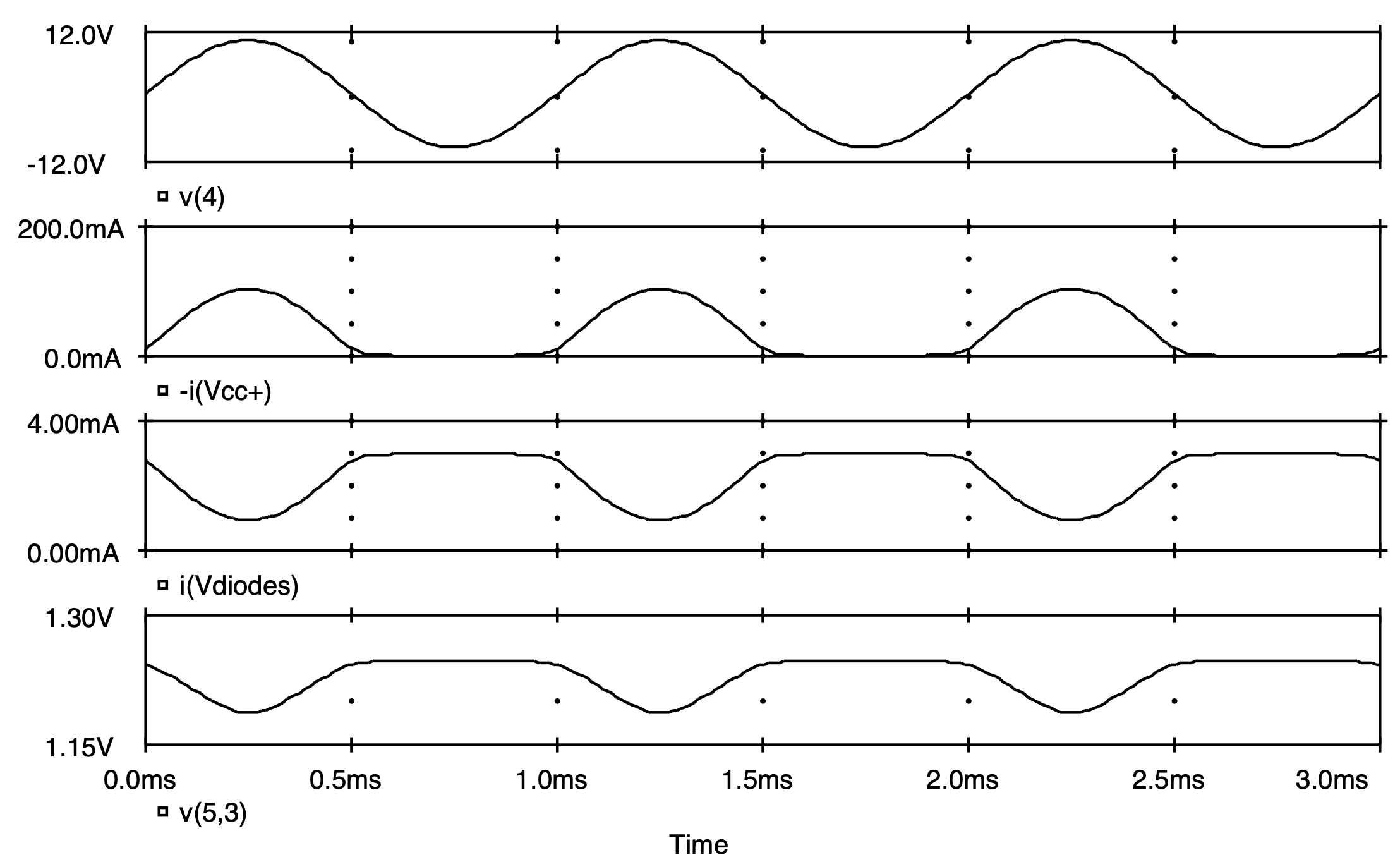
Fig. 9.15: Voltage and current waveforms of the class AB output stage. Top graph: output load voltage; second graph: collector current of QN; third graph: current through diode-connected transistors Q1 and Q2; bottom graph: bias voltage VBB.
|
9.2 Class AB Output Stage
Crossover distortion created by the output stage of an amplifier can be almost completely eliminated by a class AB configuration. In Fig. 9.13 we show a class AB output stage utilizing two diode-connected transistors (Q1 and Q2) for biasing. It is assumed that the two output transistors QN and QP are matched with IS=10-13 A and beta=50. Further, it is assumed that the QN and QP have 3 times the junction area of Q1 and Q2. Under the conditions that VCC=15 V, RL=100 Ohm, Ibias=3 mA and an input sinusoidal signal having an amplitude of 10 V and a frequency of 1 kHz, we would like to determine the variation of current through Q1 and Q2 as a function of time. In addition, we also would like to observe the voltage across the two diode-connected transistors, designated as VBB. This particular circuit was designed in Example 9.2 of Sedra and Smith where they selected the level of Ibias so that the minimum current through Q1 and Q2 never dropped be QN low 1 mA. We shall investigate whether this is indeed the case.
The Spice input file describing this class AB output stage is listed in Fig. 9.14. It is very similar to the input file used previously for the class B stage of the last section; the two major differences being that two diode-connected transistors are added, and the models for the two complementary transistors are greatly simplified. As output, the current supplied by +VCC is to be monitored which is equivalent to the collector current of QN. As well, the current flowing through the two diode-connected transistors is also to be monitored. A zero-valued voltage source Vdiodes is place in series with these two diode-connected transistors in order to accomplish this. In addition, the output voltage V(4), and V(5,3) equal to VBB are requested as output in the form of a plot.
On completion of Spice, the results of this analysis are shown in Fig. 9.15. The top graph displays the load voltage, and the graph below it illustrates the collector current of QN. Subsequently, the next graph displays the current flowing through the two diode-connected transistors Q1 and Q2. The bottom-most graph illustrates the biasing voltage VBB.
Further review of these results reveals that the minimum current through the diode-connected transistors reaches 0.94 mA, a little less than the intended design value of 1 mA. Also, the biasing voltage VBB varies between 1.25 V and 1.18 V during the time interval when QN is conducting but remains constant at 1.25 V when it is not conducting. We also see that when the output voltage is at 0 V, QN is conducting a quiescent current of 8.3 mA and the two biasing transistors Q1 and Q2 are conducting a current of 2.8 mA. The former observation suggests that the quiescent power dissipated by QN is 8.3 mA x 15 V = 124.5 mW. Likewise, the same quiescent current must be passing through QP since the output voltage is at 0 V. Thus, it too is dissipating a quiescent power of 124.5 mW. Also, the total quiescent power dissipated by the two diode-connected transistors is 2.8 mA x 1.24 V = 3.5 mW.
|
Fig. 9.16: A class AB output stage with short-circuit protection. Note that the output terminal is shorted directly to ground.
|
Class AB Output Stage With Short Circuit Protection
** Circuit Description ** * power supplies Vcc+ 1 0 DC +15V Vcc- 2 0 DC -15V Ibias 0 5 DC 3mA * input signal source Vi 3 0 sin ( 0V 10V 1kHz ) * biasing diodes (transistors connected as diodes) Q1 5 5 6 npn Q2 6 6 3 npn * output buffer (junction area of Qn and Qp is 3 times Qd1 and Qd2) Qn 1 5 7 npn 3 Qp 2 3 8 pnp 3 Re1 7 4 10 Re2 8 4 10 * short circuit protection transistor Qprotect 5 7 4 npn * short circuit output terminal Vshort 4 0 0 * simple transistor models .model npn NPN (Is=1e-13 Bf=50) .model pnp PNP (Is=1e-13 Bf=50) ** Analysis Requests ** .Tran 10us 3ms 0ms 10us ** Output Requests ** .Plot Tran V(1,7) i(Vcc+) .probe .end
Fig. 9.17: The Spice input file describing the class AB output stage shown in Fig. 9.16 having short-circuit protection.
|

|
|
|
Fig. 9.18: The top graph displays the instantaneous and average power dissipated by output transistor QN when short-circuit protected. The bottom graph displays the instantaneous and average power dissipated by QN with no short-circuit protection. As is evident, QN dissipates approximately 60% less power when protected against output short-circuit conditions.
|

9.3 Short-Circuit Protection
An important consideration of an output stage is its ability to recover from a direct short across its output terminals (i.e., hot terminal and ground). This means that the amount of current either sourced or sinked by the output stage must be limited to a safe value in order not to exceed the power limitations of the two output transistors QN and QP. In Fig. 9.16 we illustrate a simple alteration to the class AB output stage which will limit the amount of current that can be sourced by the output stage through QN. This is achieved through the addition of transistor Qprotect, and resistors RE1 and RE2.
To see the effectiveness of this approach, we shall compare the power dissipated by transistor QN with no current limiting protection to that dissipated by QN with current limiting when the output is shorted directly to ground. The input to the amplifier is assumed to be driven by a 10 V sinusoid of 1 kHz frequency. The junction area of Qprotect is assumed to be equal to one-third that of QN and QP. All other transistor parameters are assumed to be the same as those used in the previous example in section 9.3.
The Spice input deck describing the class AB output stage with short-circuit protection is given in Fig. 9.17. A transient analysis is requested to compute both the collector current of QN and its collector-emitter voltage. These two quantities are then multiplied together generating the instantaneous power dissipated by QN. The results of this analysis are shown in the top graph of Fig. 9.18. Also shown superimposed on this graph is the average power dissipated by QN. As is evident from these two curves, the peak instantaneous power is approximately 0.86 W, and the average power dissipated by QN is approximately 0.47 W.
It is interesting to compare the power dissipated by QN when it is not short-circuited protected. Consider removing Qprotect from the Spice input file listed in Fig. 9.17. Everything else remains the same. The results are then computed and displayed in the bottom graph of Fig. 9.18. As is evident, the peak instantaneous power is approximately 2 W, and the average power dissipated by QN is approximately 1 W. Thus, the short-circuit protection circuit reduced the peak instantaneous power dissipated by QN by 60% and the average power dissipated by 56%. An even greater power reduction is possible by increasing the value of the two emitter resistors RE1 and RE2. But, of course, this decreases the effective voltage swing of the output stage.
9.4 Spice Tips
· The current through a resistor is directly accessible in PSpice. No zero-valued voltage source is required to be placed in series with the resistor. This simplifies the creation of the input Spice deck.
· The Fourier Analysis command of Spice decomposes a time-domain waveform into its Fourier series components. This includes the fundamental, a DC component and the next eight harmonics. In addition, a total harmonic distortion measure (THD) is also provided.
· Fourier analysis is performed on the last cycle of a time-varying waveform computed by Spice. It is therefore important that by the final cycle the waveform has reached steady state if the Fourier analysis results are to be interpreted correctly.
· Amplifier power efficiency can be computed using the results obtained through a transient analysis, i.e., voltages and currents. The post-processing capabilities of Probe are helpful in generating graphical displays of the various power waveforms by multiplying different voltage and current signals together and by computing a running average.
9.5 Problems
9.1. A class A emitter follower, biased as in Fig. 9.1, uses VCC=5 V, R=RL=1 k-ohm, with all transistors (including Q3) identical. Assume beta is very large. For linear operation, what are the upper and lower limits of the output voltage, and the corresponding inputs? How do these values change if the emitter-base junction area of Q3 is made twice as big as that of Q2. Half as big? Repeat for beta=50.
9.2. A source-follower circuit using enhancement NMOS transistors is constructed following the pattern shown in Fig. 9.1. All three transistors used are identical with Vt=1 V and un COX=20 mA/V2. In addition, VCC=5 V, R=RL=1 k-ohm. For linear operation, what are the upper and lower limits of the output voltage, and the corresponding inputs?

P9.3
9.3. The BiCMOS follower shown in Fig. P9.3 uses devices for which IS=100 fA, beta=100, un COX=20 mA/V2, and Vt=-2 V. For linear operation, what is the range of output voltages obtained with RL=infinity as calculated by Spice? With RL=100 Ohm? What is the smallest load resistance allowed for which a 1 V peak sine-wave output is available? What is the corresponding power-conversion efficiency?
9.4. Consider the feedback configuration with class B output shown in Fig. P9.4. Let the amplifier gain A0=100 V/V and the bipolar transistors be modeled after the NA51 and NA52 commercial transistors. Spice parameters for these devices can be obtain from Fig. 9.8. Compute the input-output voltage transfer characteristics using Spice. Compare these results to those generated by Spice for a corresponding class B output stage without feedback.

P9.4
9.5. For the feedback amplifier shown in Fig. P9.4, with pertinent parameters described in Problem 9.4, compute the output voltage transient waveform for an input 5 kHz sine-wave voltage signal of 6 V peak using Spice. Also, have Spice compute the Fourier Series coefficients of this output signal. What is the resulting Total Harmonic Distortion (THD) of this amplifier? Repeat the analysis on a corresponding class B output stage without feedback present. How do the THD results compare?

P9.6
9.6. Consider the class B output stage using enhancement MOSFETs shown in Fig. P9.6. Let the devices have |Vt|=1 V and unCOX=2upCOX= 200 mA/V2. With a 10 kHz sinewave input of 5 V peak and a high value of load resistance, what peak output results? What fraction of the sine-wave period does the crossover interval represent? For what value of load resistance is the peak output voltage reduce to half the input?
9.7. Consider the complementary BJT class B output stage constructed from 2N2222A commercial transistors. (See section 9.1 for Spice model parameters). For ±10 V power supplies and a 100 Ohm load resistance, what is the maximum sine-wave output power available? What is the power conversion efficiency? For output signals of half this amplitude, find the output power, the supply power, and the power-conversion efficiency.
9.8. A class AB output stage using a two-diode bias network as shown in Fig. 9.13 utilizes diodes having the same junction area as the output transistors. For VCC=10 V, Ibias=0.5 mA, RL=100 Ohm and beta=50, what is the quiescent current computed by Spice when the output is at 0 V? How much power is dissipated by this output stage?

P9.9
9.9. The circuit shown in Fig. P9.9 uses four matched transistors for which IS=10 fA and beta ³ 50. What quiescent current flows in the output transistors? What bias current flows in the bases of the input transistors? Where does it flow? What is the net input current (the offset current) for a beta mismatch of 10%? For a load resistance RL=100 Ohm, what is the input resistance? What is the small-signal voltage gain?
9.10. Characterize a Darlington compound transistor formed from two npn BJTs modeled after the 2N3904 commercial transistor using Spice. For operation at 10 mA, what is the equivalent VBEeq, rpeq and gmeq?
9.11. The circuit shown in Fig. P9.11 operates in a manner analogous to that in Fig. 9.16 to limit the output current from Q3 in the event of a short circuit or other mishap. With the aid of Spice, determine the value of R that causes Q5 to turn on and absorb all of Ibias=2 mA when the current being sourced reaches 150 mA. Assume that all devices can be described by IS=10-14 A and beta=100. If the normal peak output current is 100 mA, find the voltage drop across R and the collector current in Q5.
9.12. For the current conveyor circuit shown in Fig. P9.12, assuming all transistors to have large beta and Ao=106, compute the output current io when the output is shorted directly to ground using Spice. Compare this to the situation where beta=100. By what percentage has io changed? The diodes are meant to be realized using a diode-connected transistor.

P9.11

P9.12